

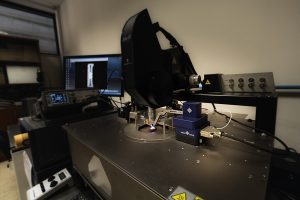
 How do you test the sensors in smartphones, smartwatches, and up-and-coming medical devices? With a Femtotools FT-RS1002 Microrobotic System of course! In 2016 the Department of Microelectronics and Nanoelectronics (Faculty of ICT, UoM) set up a slew of devices to be able to to probe, prod and poke devices up to a resolution of 1 nm (thinner than the diameter of a human hair).
| Quick Specs |
|
Number of axes: 3 Maximum velocity: 5 mm/s Minimum motion increment: 1 nm Actuation principle: Piezoelectric scanning/stepping Sensor probe tip area: 50 µm x 50 µm FT-S100000 sensor force range: ±100000 µN FT-S100000 sensor resolution at 10Hz: ±5 µN Operating temperature: 5°C to 100°C |
The team of computer scientists collaborated with global semiconductor chip maker ST Microelectronics to p roduce MEMS (Micro-Electro-Mechanical Systems). MEMS are the tiny sensors or devices often found in smartphones that allow them to act like a compass, know how fast a person is going, or detect sound. In Malta, the new equipment is being used to measure mechanical properties (for example shear testing and flexure testing) of tiny mirrors that can be used to turn phones into high-quality projectors (part of the Lab4MEMS2 project part-funded by the EU). This toolkit is incredibly versatile, forming part of a station that can have additional add-ons to widen its applications. Now the team wants to buy more sensitive microforce probes and microgrippers that will allo w the manipulation and assembly of microsystems. This toolkit’s micromechanical testing can be used in many research and industrial applications. This way, the horizon is open for studies into semiconductor technology, microsystem development, materials science, micromedicine, or biotechnology—placing Malta on the semiconductor map.


 “My summer experience at
 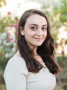 ʻThe months spent at CERN for the summer student internship programme were not only an invaluable experience, but also an insight to future potential careers for my colleagues and I. Based within the HMPID detector of the ALICE experiment, we had a six-week lecture program focused on the fundamental properties of nature. The bulk of the work we were involved in centred on implementing programming languages to process raw data from collisions into useful knowledge. Geneva provided a change of pace for us that was conducive to both hard work and extra curricular activities. Travelling across borders, visiting main projects and control centres at CERN, while also socialising with students from all over the globe, made it an all-encompassing experience not easily matched.ʼ
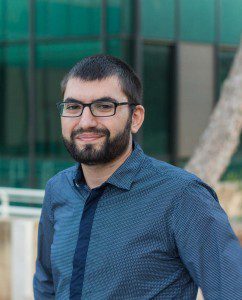 The HMPID takes snapshots of the faint patterns generated by the high-energy collisions, passing this information through the RICH electronics module which cleans and transforms it for analysis. Magri is working to optimise the electronic circuits and control boards to improve how data is handled. So far, he has manipulated computer processes to create parallelism, allowing for processes that previously happened one after the other to occur simultaneously. He also used high-throughput interconnects, which, when coupled with parallelism, are expected to increase data collection tenfold. Magri’s work will be combined with that of other researchers and integrated by 2020 in order to improve the detector’s accuracy, potentially revealing building blocks of matter that might have yet to be seen.
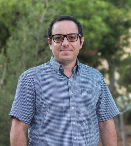 Working in close collaboration with Magri, Seguna is developing novel electronic circuitry for the CPV and HMPID detectors, that will boost the speed at which collisions are read, going from 4 kHz to 50 kHz, the speed at which the beams interact: true real time. Seguna’s research will be taken on at CERN between 2020–2023.
