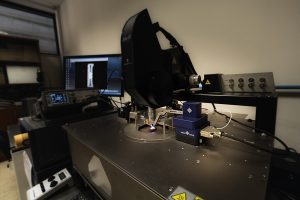
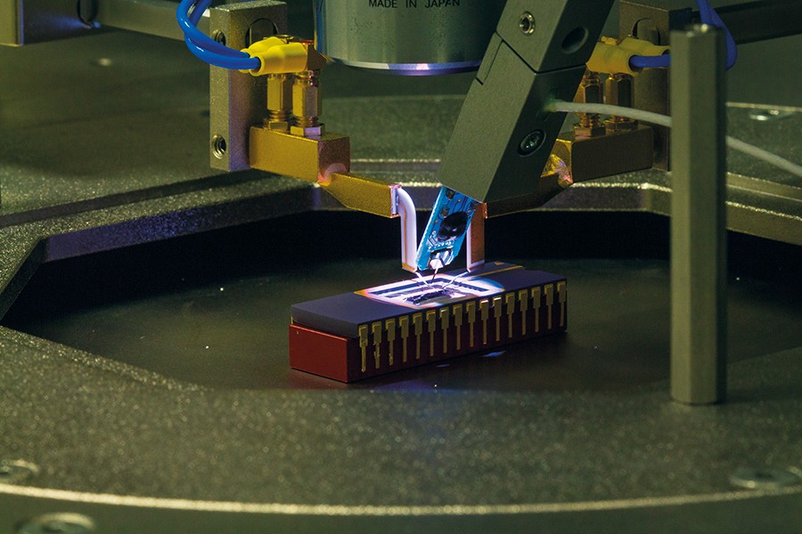
 How do you test the sensors in smartphones, smartwatches, and up-and-coming medical devices? With a Femtotools FT-RS1002 Microrobotic System of course! In 2016 the Department of Microelectronics and Nanoelectronics (Faculty of ICT, UoM) set up a slew of devices to be able to to probe, prod and poke devices up to a resolution of 1 nm (thinner than the diameter of a human hair).
| Quick Specs |
|
Number of axes: 3 Maximum velocity: 5 mm/s Minimum motion increment: 1 nm Actuation principle: Piezoelectric scanning/stepping Sensor probe tip area: 50 µm x 50 µm FT-S100000 sensor force range: ±100000 µN FT-S100000 sensor resolution at 10Hz: ±5 µN Operating temperature: 5°C to 100°C |
The team of computer scientists collaborated with global semiconductor chip maker ST Microelectronics to p roduce MEMS (Micro-Electro-Mechanical Systems). MEMS are the tiny sensors or devices often found in smartphones that allow them to act like a compass, know how fast a person is going, or detect sound. In Malta, the new equipment is being used to measure mechanical properties (for example shear testing and flexure testing) of tiny mirrors that can be used to turn phones into high-quality projectors (part of the Lab4MEMS2 project part-funded by the EU). This toolkit is incredibly versatile, forming part of a station that can have additional add-ons to widen its applications. Now the team wants to buy more sensitive microforce probes and microgrippers that will allo w the manipulation and assembly of microsystems. This toolkit’s micromechanical testing can be used in many research and industrial applications. This way, the horizon is open for studies into semiconductor technology, microsystem development, materials science, micromedicine, or biotechnology—placing Malta on the semiconductor map.


Comments are closed for this article!