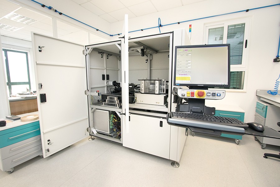
Silicon is the go-to material for solar devices like photovoltaic panels despite its relatively low energy conversion rate of 15-22%. Researchers all over the world are analysing materials and creating new ones to find a better solution. A lucky handful are armed with a laser scattering tomograph (LST), the best instrument for the task.
An LST illuminates the sample material with an infrared laser beam, which scatters wherever it finds a defect. If there is a defect in a material’s structure, even one just a few nanometers wide, the very sensitive CCD camera at the other end of the machine will pick it up, allowing researchers to learn and adapt. It also boasts a robotic system that allows it to automatically load multiple samples at once.
The LST is very rare, but fortunately, one has found a home at the University of Malta’s (UM) Institute for Sustainable Energy (ISE), a brand new, state-of-the-art facility aimed towards finding efficient solutions for harnessing solar power to its fullest extent. ‘There are probably 10 to 12 of these worldwide,’ confirms Prof. Luciano Mule’ Stagno, Director of the Lab at the ISE. ‘Ours is one of the few in the world to be found in a university, almost certainly the only one in a university in Europe. Most of these machines are in industry settings,’ he says.
This enables the UM to conduct cutting-edge research in a field that is practically nascent, putting it at the forefront. With the LST, material engineers could unlock the secrets behind the perfect variation of defect-reduced silicon. This rise in efficiency could have a substantial impact on the worldwide sustainable energy market.


Comments are closed for this article!